This is a quick guide to getting a totally dead Oric mainboard to some level of "working". Read it in conjunction with the Oric Schematic diagram (Oric Owner Issue 5, Advanced User Guide by L. Whewell) and the Oric Service Manual.
Any specific questions on this document by email to oric@signal11.org.uk
Note: The Oric Service manual suggests tests in an order which is likely to result in a lot of chip changing and probing before finally reaching page 37 where the important "is there any power?" question is asked. This document is laid out in what I feel is a more logical progression of tests, working from highest dependency to lowest.
Guide currents and measurements may vary from system to system, and may vary with the test equipment used. They are included only for guidance.
The diagnostic ROM mentioned and external diagnostic board should be available from the same place you found this document (oric.signal11.org.uk).
Where ICs are removed for testing or replacement, fit a DIL socket – it will make future repairs or tests much easier and reduce the risk of damage to the PCB traces.
// 1: VISUAL CHECKS
Don't overlook the obvious!
- Physical damage to tracks, components, soldered joints. Bent pins on keyboard connector, printer port, expansion port.
- Missing parts. Exclude IC10 and IC11 which are either both fitted (early Oric), or both missing (most boards).
- Partly completed/incorrectly applied service bulletins/modifications.
- Other non-standard modifications.
// 2: VERIFY POWER SUPPLY
Without a working power supply, none of the other testing can be carried out.
- Remove ULA and Oric ROM from sockets and store them.
- Check 5v-0v rail resistance against known good board (approx 225R). If lower than 50R skip powering up and go straight to step 2.4
- Power up from a current limited PSU (9V DC/Max 700mA, DC Jack centre positive). If 5v rail is 4.95v to 5.05v, power supply is good, return ULA to socket, and go to section 3.
- See the 7905 photo below. Check C8 next to the DC input jack is not short circuit (replace if needed). Unsolder and lift the "OUT" leg of 7905 from board or cut trace as shown. If +5v is not present between separated (0v) "OUT" and (+5v) "COM" leg, unbolt and replace 7905. Go back to step 2.2 and start again.
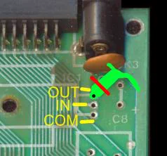
01_0vRail_7905 – 7905 regulator, "OUT" leg separated - Separate entire DRAM 0v supply (see the DRAM photo below, 2 PCB cuts at 'A'). Recheck rail resistance and with power applied, total current and rail voltage. If fault clears, one or more DRAM chip is probably faulty, continue to next step. Else go to step 2.8
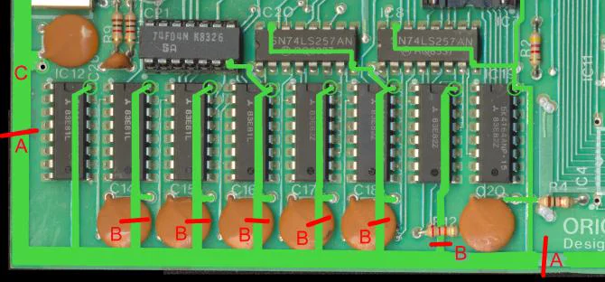
02_0vRail_DRAM_Detail – DRAM 0v rail cuts 'A' and 'B', ground point 'C' - Separate individual DRAM 0v supply (see the DRAM photo above, 6 PCB cuts, some under capacitors, at 'B'). With power applied, check current from actual ground at point 'C' to each DRAM chip pin 16 (marked with circle), which should be about 4mA. Anything over 100mA is a suspect chip. IC 15, 17, 19 may read slightly higher (up to 30mA) than the others due to shared 0v rail with IC21, 20, 8 above them, this is normal.
- Remove all suspect DRAM chips identified from step 6 above. Important: test current draw of chip out of circuit with a separate power supply +5v to pin 8, 0v to pin 16 (reversed from normal TTL pinning!). If current is over 80mA discard chip. If current is lower, chip may be reusable – test it in known good system before deciding on discarding or re-using. On IC 15, 17 and 19 – if the current is acceptable when taken out of circuit, double check the current from point 'C' to pin 16 of the NOW EMPTY DRAM IC position for possible fault on neighbouring IC21, 20, 8 (and remove those if necessary). Then go back to step 2.2 and start again.
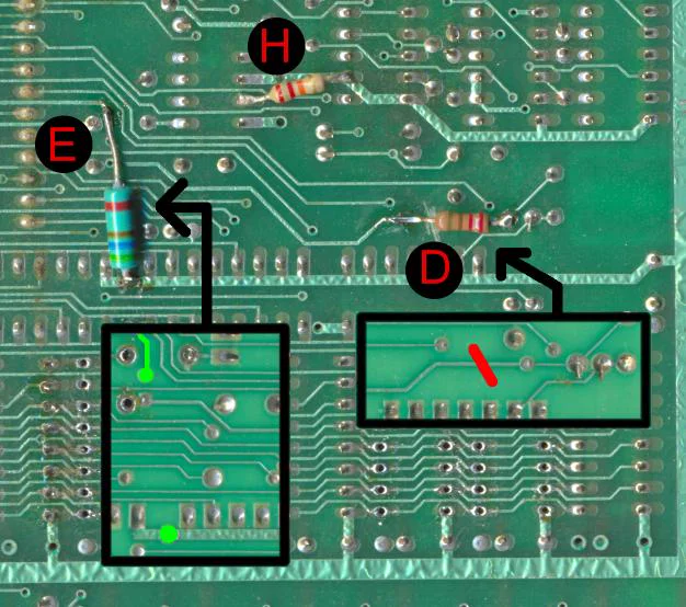
- Separate power supplies of CPU/ROM (see the CPU/VIA/PSG photo below, 2 PCB cuts at 'D'). ROM should not be installed at this point. Recheck rail resistance and with power applied, total current and rail voltage. Check current from ground at point 'C' to pin 1 of CPU. If fault clears CPU may be faulty, continue to next step. Else go to step 2.10
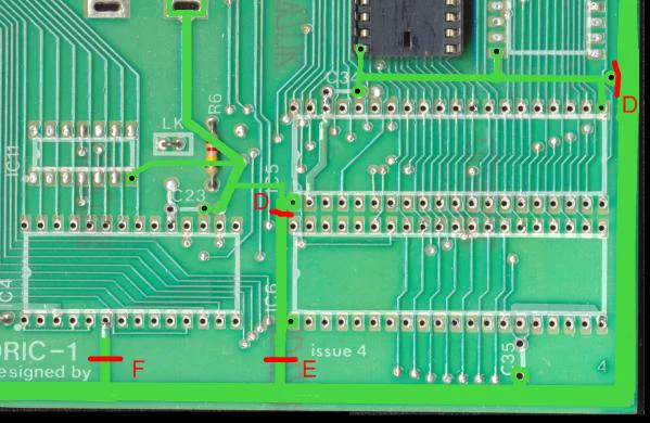
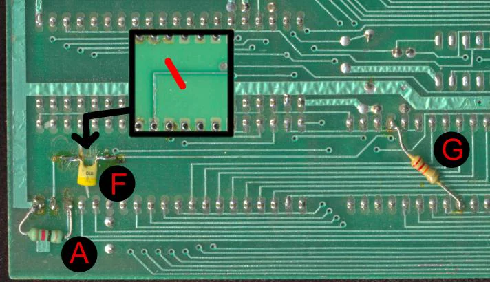
03_0vRail_CPUVIAPSG_Detail – CPU/ROM cuts 'D', VIA cut 'E', PSG cut 'F' - Remove suspect CPU. Test current of chip out of circuit with a separate power supply +5v to pin 8, 0v to pin 1 and 21. If current is significantly over (150mA) discard chip. Otherwise test in a known good system before discard or re-use. Go back to step 2.2 and start again.
- Separate power supply of VIA (see the CPU/VIA/PSG photo above, 1 PCB cut at 'E'). Recheck rail resistance and with power applied, total current and rail voltage. Check current from ground at point 'C' to pin 1 of VIA. If fault clears, VIA may be faulty, continue to next step. Else go to step 2.12
- Remove suspect VIA. Test current of chip out of circuit with a separate power supply +5v to pin 20, 0v to pin 1. If current is significantly over 70mA discard chip. Otherwise test in a known good system before discard or re-use. Go back to step 2.2 and start again.
- Separate power supply of PSG (see the CPU/VIA/PSG photo above, 1 PCB cut at 'F'). Recheck rail resistance and with power applied, total current and rail voltage. Check current from ground at point 'C' to pin 6 of PSG. If fault clears, PSG may be faulty, continue to next step. Else go to step 2.14
- Remove suspect PSG. Test current of chip out of circuit with a separate power supply +5v to pin 3 and 19, 0v to pin 6. If current is significantly over 70mA discard chip. Otherwise test in a known good system before discard or re-use. Go back to step 2.2 and start again.
If there is still a power supply fault:
Make further cuts to the 0v rail to isolate inner sections of the board to narrow down the fault to a particular area (see the full board view below). Check that cutting the trace has actually isolated the area – there are some loops in tracks in the upper left corner of the PCB toward the UHF modulator.
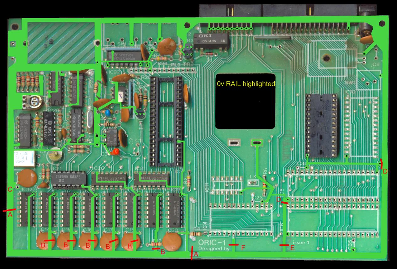
In each case if the fault clears, and the 5v rail returns, the fault is "beyond" the cut track. Prove this by checking current from an actual ground point to the other side of the last cut trace. None of the remaining chips draw significant current in normal operation, any heavy load found at this stage is the fault.
Once the power supply is correct at 5v:
Replace any chips removed above with sockets to make later repairs easier.
Insert known good chips for any removed items above. Any chips that were removed and tested as OK in another board can be returned.
Repair any PCB cuts made above by clearing a small amount of solder resist either side and soldering across the gap. Ensure rail is still at +5v once replacement chips are inserted.
Reinstall the ULA but not the ROM.
// 3: VERIFY CLOCKS
The PCB should now have 5v present, drawing under 600mA total. Next ensure that all timing signals are operating as without timing signals it is impossible to test further.
The following TTL clocks must be present, check with an oscilloscope, frequency counter or logic probe:
- Ensure 12 MHz clock available at source pin 2 IC21 and destination pin 7 ULA.
- Ensure 1MHz clock available at source pin 14 ULA and destination pin 37 CPU.
- Ensure 1MHz clock available at source pin 3 CPU and destination pin 15 PSG.
- Ensure 1MHz clock available at source pin 39 CPU and destination pin 25 VIA, pin 5 IC21.
- Ensure 1MHz clock available at source pin 6 IC21 and destinations pin 22 IC9, pin 22 IC10.
If any clock is entirely missing, low in level, or off frequency, cut the trace between source and destination. Now identify whether the source is failing to provide a clock (still no clock present) OR the destination is overloading clock (clock returned).
Check for damage to traces or accidental short circuit on traces to neighbouring pins, tracks or a thru-hole before suspecting the ICs.
Finally replace IC21, ULA, CPU, PSG or VIA as necessary from above tests until all clocks are present. Repair any PCB cuts made for testing.
- Ensure 8.86MHz clock available at IC25 pin 10, 12 and 4 to IC24 pins 11 and 3
- Ensure 4.43MHz clock available at IC24 pins 8, 12 and 5 to IC23 pins 5 and 6.
Correction (2021/02/04): step 7 originally read "8.86MHz clock"; it should read "4.43MHz clock".
Replace IC25 or IC24 as necessary. IC23 is a custom PROM. To replace it, spares must be salvaged from other ORICs or 24S10 (256x4) PROM can be programmed with dump from appendix in L. Whewell's Advanced User Guide.
Once all clocks are established, go on to next section.
// 4: CHECK SYSTEM ADDRESS/DATA BUS
Now that there is a chance the system can start up, fit the diagnostic ROM/diagnostic board. The first test is a RAM test which proves out the CPU/ULA/ROM link. If the RAM test executes (whether it passes or fails) there will be continuous pulsed activity on the data bus (D0-D7), and the address bus will be cycling (A0 and A1 rapidly pulsing, possibly other higher address lines). If this is the case, go onto the next section.
If there is no activity on the address and data lines, check D0-D7 and A0-A15 of the system buses as described in the Service Manual p35-37 for lines that are stuck high or low. Remember that CPU is the source of lines A0-A15, all other devices are a load. Replace any defective ICs with socketted parts, and repeat until RAM test passes (or fails with an endless loop of bus activity).
An alternative strategy is to remove the ULA (socketted) and test just the CPU to ROM operation. This can only be easily done with the external diagnostic board in place. With the diagnostic board fitted, use the external 1MHz clock lead to pin 14 of the empty ULA socket. This should cause a RAM test to be performed which will FAIL leaving the CPU cycling endlessly.
If the status LEDs are fitted to the diagnostic board, a status code of "1" (A7-A2 set to 000001) should be seen. Also regular pulses should be found on the CPU SYNC pin (pin 7) indicating opcode fetches from ROM. Phi 1 and Phi 2 clocks (pin 3 and 39) should be 1MHz waves. If this is not the case the CPU is not able to function – either it is faulty or the address and data lines are blocked.
// 5: APPLY ESSENTIAL SERVICE BULLETINS/MODIFICATIONS
See Oric Service Manual for full details. Fitting and removing of supply decoupling capacitors skipped.
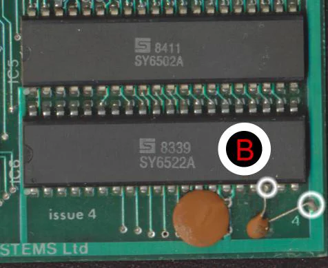
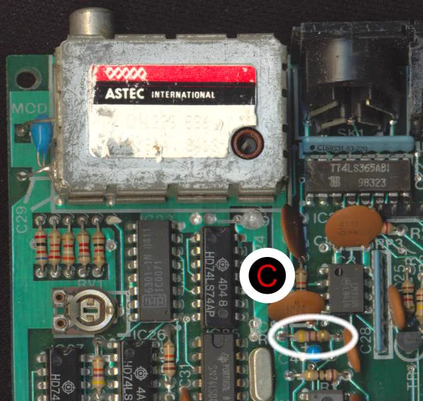
See the four photos below for physical locations.
- Ensure modification 52/53/56 fitting/removal of parts ended up as both parts FITTED.
Cassette reliability: Pin 18 VIA 1K resistor to +5v (bottom side) at 'A'; 2n2 capacitor to 0v (top side) at 'B'.
Also PSG Volume: Remove R3 at 'C'. [MJB: Too loud! Optionally: Replace R3 with 1K5-4K7, higher value = higher volume] - Ensure modification 63b fitted.
Startup reliability: Cut track from IC21 pin 2 at 'D', insert 220R resistor. Add 560R resistor from ULA pin 7 to +5v at 'E'. - Ensure Service Bulletin 1 performed on ORIC mainboards. (Not needed for ATMOS)
PSG BDIR Pulse length fix: Cut track from pin 19 VIA at 'F', bridge gap with 1n0 capacitor. 22K Resistor from PSG pin 18 to pin 6 at 'G'. - Ensure modification from service manual (no identifier) performed.
Add 22K resistor from pin 3 IC2 to pin 9 IC25 (ground) at 'H'.
// 6: RUN DIAGNOSTICS ROM
- To check correct operation of ULA, RAM, VIA, PSG and all related support circuitry, run the diagnostic ROM as per the instructions with it.
- If a test fails, further fault finding will be needed around the indicated area of the mainboard, refer to diagnostic ROM instructions for specific test details and the Oric Service manual for some other hints:
Screen faults (RGB out, UHF out or both): p26-29
Picture quality: p30
Sound faults: p31
Keyboard faults: p32-34, 40
// 7: SOAK TEST
- If the diagnostic test now passes, fit the keyboard and remount all parts into case.
- Use the diagnostic ROM ULA test cards to check alignment and frequency of UHF output on Channel E-36 for best picture.
Adjust RV1 so that the yellow part of the test card just starts to turn white.
Adjust CV1 for least colour fringing on text once Oric is warmed up and stabilized.
If Diagnostic ROM used internally, return original ORIC ROM. Otherwise disconnect Diagnostic ROM board from expansion port.
© 2008 Mike Brown. Reproduced with credit to oric.signal11.org.uk, where the original checksheet, photos, diagnostic ROM and diagnostic board can be found.